Author:
bhasker
[ Edit | View ]
|
Date Posted: 05:29:31 12/18/03 Thu
Author Host/IP: NoHost/202.138.112.241
Although i usually dont encounter too much of electronics apart from maybe my third semester subject "digital systems " which was quite an eye opener (author praises Anna University for selecting a few nice subjects in our syllabus!) ... the search for a practical way of setting up the whooe circuit from scratch has been daunting. I havnt been able to find the components for making nuthin ... and it is in this haste and frustration that i searched and found ...well the text you will be reading below !!

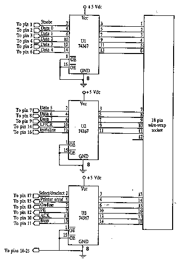
This is about the most basic interface you will see. It uses only 3 74376's (74LS367). This interface provides 8 outputs (plus 3 address lines) and 5 inputs. This is usually enough for one room, providing you make use of some demultiplexers and the address lines. You could have up to 128 output lines using the address lines, a 74LS138 and 8 74LS154's.
Begin construction by mounting the IC sockets on the board. I used a experimenters universal solder board due to the large number of wires that must cross. If a PC board were used, you would need either a multi-layer board or many, many jumpers.
Now, solder wires along the top and bottom of the board, making all the connections between the IC sockets. Do not install the IC's yet. Assemble the cable using 26 conductor ribbon cable and a 25 pin crimp connector. You will have one conductor left over so just "peel" it off. Connect the cable to the board and wire it into the circuit. I used an 18 pin socket to make connections to the outputs and inputs on the interface easy. You could do the same if you like, or use a terminal strip.
Schematic Of The Parallel Port Interface
pcb software downloads here
Simple circuit and program to show how to use PC parallel port output capabilities
PC parallel port can be very useful I/O channel for connecting your own circuits to PC. The port is very easy to use when you first understand some basic tricks. This document tries to show those tricks in easy to understand way.
WARNING: PC parallel port can be damaged quite easily if you make mistakes in the circuits you connect to it. If the parallel port is integrated to the motherboard (like in many new computers) repairing damaged parallel port may be expensive (in many cases it it is cheaper to replace the whole motherborard than repair that port). Safest bet is to buy an inexpensive I/O card which has an extra parallel port and use it for your experiment. If you manage to damage the parallel port on that card, replacing it is easy and inexpensive.
DISCLAIMER: Every reasonable care has been taken in producing this information. However, the author can accept no responsibility for any effect that this information has on your equipment or any results of the use of this information. It is the responsibly of the end user to determine fitness for use for any particular purpose. The circuits and software shown here are for non commercial use without consent from the author.
How to connect circuits to parallel port
PC parallel port is 25 pin D-shaped female connector in the back of the computer. It is normally used for connecting computer to printer, but many other types of hardware for that port is available today.
Not all 25 are needed always. Usually you can easily do with only 8 output pins (data lines) and signal ground. I have presented those pins in the table below. Those output pins are adequate for many purposes.
pin function
2 D0
3 D1
4 D2
5 D3
6 D4
7 D5
8 D6
9 D7
Pins 18,19,20,21,22,23,24 and 25 are all ground pins.
Those datapins are TTL level output pins. This means that they put out ideally 0V when they are in low logic level (0) and +5V when they are in high logic level (1). In real world the voltages can be something different from ideal when the circuit is loaded. The output current capacity of the parallel port is limited to only few milliamperes.
Dn Out ------+
|+
Sourcing Load (up to 2.6 mA @ 2.4 v)
|-
Ground ------+
Simple LED driving circuits
You can make simple circuit for driving a small led through PC parallel port. The only components needed are one LED and one 470 ohm resistors. You simply connect the diode and resistor in series. The resistors is needed to limit the current taken from parallel port to a value which light up acceptably normal LEDs and is still safe value (not overloading the parallel port chip). In practical case the output current will be few milliampres for the LED, which will cause a typical LED to somewhat light up visibly, but not get the full brigtness.

Then you connect the circuit to the parallel port so that one end of the circuit goes to one data pin (that one you with to use for controlling that LED) and another one goes to any of the ground pins. Be sure to fit the circuit so that the LED positive lead (the longer one) goes to the datapin. If you put the led in the wrong way, it will not light in any condition. You can connect one circuit to each of the parallel port data pins. In this way you get eight software controllable LEDs.
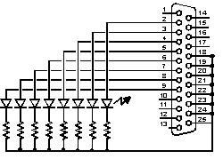
The software controlling is easy. When you send out 1 to the datapin where the LED is connected, that LED will light. When you send 0 to that same pin, the LED will no longer light.
Parallel port controlling in Linux , and original fource bhasker suggests that u click
here
Controlling some real life electronics
The idea of the interface shown above can be expanded to control some external electronics by simply adding a buffer circuit to the parallel port. The programming can be done in exactly the same way as told in my examples.
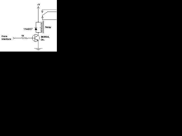
Building your own relay controlling circuit
The following circuit is the simples interface you can use to control relay from parallel port:
Vcc
|
+------+
| __|__
Relay /^\ Diode 1N4002
Coil /---\
| |
+------+
|
| /
4.7K B |/ C
parallel port >-\/\/\/\/---| NPN Transistor: BC547A or 2N2222A
data pi |\ E
| V
|
parallel port >--------------+
ground pin |
Ground
The circuit can handle relays which take currents up to 100 mA and operate at 24V or less. The circuit need external power supply which has the output voltage which is right for controlling the relay (5..24V depending on relay). The transistor does the switching of current and the diode prevent spikes from the relay coil form damaging your computer (if you leave the diode out, then the transistor and your computer can be damaged).
Since coils (solenoids and relay coils) have a large amount of inductance, when they are released (when the current is cut off) they generate a very large voltage spike. Most designs have a diode or crowbar circuit designed to block that voltage spike from hitting the rest of the circuit. If that diode is bad, then the voltage spike might be destroying your "sink" transistor or even your I/O card over a period of time. The mode of failure for the sink transistor might be short circuit, and consequently you would have the solenoid tap shorted to ground indefinitely.
The circuit can be also used for controlling other small loads like powerful LEDS, lamps and small DC motors. Keep in mind that those devices you plan to control directly from the transistor must take less than 100 mA current.
WARNING: Check and double check the circuit before connecting it to your PC. Using wrong type or damaged components can cause you paralllel port get damaged. Mistakes in making the circuit can result that you damage your parallel port and need to buy a new multi-io card. The 1N4002 diode in parallel with the relay is an essential protection component and it should not be left out in acu case, or a damage of the parallel port can occur because of high voltage inductive kickback from the relay coil (that diode stops that spike from occuring),
Safer new design
The circuit example above works well and when transistor is of correct type and working properly. If for some reason B and C sould be shorted together and you are suing more than +5V in the relay side, the circuit can push that higher voltage to the parallel port to damage it. The following circuit uses two 1N4148 diodes to protect parallel port against higher than +5V signals and also against wrong polarity signals (power on the circuit is accidentally at wrong polarity.
Vcc
|
+------+
| __|__
Relay /^\ Diode 1N4002
Coil /---\
| |
+------+
|
Diode | /
1N4148 4.7K B |/ C
parallel >-|>|-+--\/\/\/--| NPN Transistor: BC547A or 2N2222A
port data | |\ E
pin +-|<|-+ | V
1N4148 | |
parallel >-----------+------+
port ground |
Ground
Adding even more safety idea: Repalce the 1N4148 diode connected to ground with 5.1V zener diode. That diode will then protect against overvoltage spikes and negative voltage at the same time.
Bad circuit example
I don't know WHY I see newbies who don't THINK electronics very well yet always putting the relay "AFTER" the transistor, as if that was something important. Well it's NOT, and in fact its a BAD PRACTICE if you want the parallel port to work well! This type of bad circuit designs have been posted to the usenet electronics newsgroups very often. The following circuit is example of this type of bad circuit design (do not try to build it):
Vcc
|
| /
4.7K B |/ C
parallel port---\/\/\/\/---| NPN Transistor: BC547A or 2N2222A
|\ E
| V
|
+------+
| __|__
Relay /^\ Diode 1N4002
Coil /---\
| |
+------+
|
Ground
NOTE: This is a bad design. Do not build or use this circuit.
The problem of the circuit is that the voltage which goes to the relay is always limited to less than 4.5V even if you use higher Vcc supply. The circuit acts like an emitter follower, which causes that the voltage on the emitter is always at value base voltage - base to emitter voltage (0.6..0.7V). This means that with maximum of 5.1V control voltage you will get maximum of 4.5V out no matter what is the supply voltage (when it higher than 5V and below transistor breakdown voltage).
Other problem is that in some cases this type of circuit can start to oscillate if the base resistor is right on the edge.
Circuit with optoisolation
If you want to have a very good protection of the parallel port you might consider optoisolation using the following type of circuit:
V+ (12V)
|
+------------+
| +------+
Parallel | | |
Port | D1 --- |
| 1N4001 / \ Relay coil
R1 1 ----------- 5 | /---\ |
D(x) ----1k------| Opto- |-----+ | |
| Isolator | +------+
GND -------------| |-+ |
2 ----------- 4| |
CNY 17 or | R2 | /
4N25 | 4.7K B |/ C T1
+--\/\/\/\/---| BC547A or 2N2222A
|\ E
| V
|
external circuit ground
Typical optoisolator pinout (CNY 17 and 4N25):
-----------------------------
1--|---- |------------|--6
| | | |
| \---/ \ | ------ |
| \ / \ | | / C | |
| --- \ \| | |/ | |
| | \ -- --| ---|--5
| | \| B |\ |
2--|---- -- | V E |
| --------|--4
3--|--NC |
-----------------------------
The opto-isolator is there to protect the port. Note that there are no connections between the port's electrical contacts. The circuit is powered from external power supply which is not connected to PC if there is no need for that. This arrangement prevents any currents on the external circuits from damaging the parallel port.
The opto-isolator's input is a light emitting diode.R1 is used to limit the current when the output from the port is on. That 1kohm resistor limits the current to around 3 mA, which is well sufficent for that output transitor driving.
The output side of the opto-isolator is just like a transistor, with the collector at the top of the circuit and the emitter at the bottom. When the output is turned on (by the input light from the internal LED in the opto-coupler), current flows through the resistor and into the transistor, turning it on. This allows current to flow into the relay.
Turning the input on the parallel port off causes the output of the opto-isolator to turn off, so no current flows through it into the transistor and the transistor turns off. When transistor is off no current flows into the relay, so it switches off. The diode provides an outlet for the energy stored in the coil, preventing the relay from backfeeding the circuit in an undesired manner.
The circuit can be used for controlling output loads to maximum of around 100 mA (depends somewhat on components and operation voltage used). The external power supply can be in 5V to 24V range.
Optoisolated higher power circuit
Here is a higher power version of the circuit described above:
V+ (12V)
|
+------------+-----+------+
| | |
Parallel | | |
Port | D1 --- |
| 1N4001 / \ Relay coil
R1 1 ----------- 5 | /---\ |
D(x) ----1k------| Opto- |-----+ | |
| Isolator | +-----+------+
GND -------------| |-+ | |
2 ----------- 4| | |
CNY 17 or | R2 | / |
4N25 | 4.7K B |/ C T1 |
+--\/\/\/\/---| BC547A |
| |\ E |
| | V | /
/ | B |/C T2
\ R3 +----------| power
/ 10 kohm |\E transistor
\ | v
| |
+----------------------------+
|
external circuit ground
In this circuit Q1 is used for controlling the base current of Q2 which controls the actual current. You can select almost any general purpose power transistor for this circuit which matches your current and voltage controlling needs. Some example alternatives are for example TIP41C (6A 100V) or 2N3055 (100V 15A). Depending your amplification facter inherint to the transitor Q2 you might not hough be able to use the full current capability of the output device T2 before there will be excessive losses (heating) in that transistor.
This circuit is basically very simple modification of the original optoisolator circuit with one transistor. The difference in this circuit is that here T2 controls the load current and Q1 acts as a current amplifier for T2 base control current. Optoisolator, R1, R2, Q1, D1 work exactly in the same way as in one transistor circuit described eariler in this documents. R3 acts like an extra resistor which guarantees that T2 does not conduct when there is no signal fed to the optoisolator (small possible current leaking on optosiolator output does not make T1 and T2 to conduct).
Reading the input pins in parallel port
PC parallel port has 5 input pins. The input pins can be read from the I/O address LPT port base address + 1.
The meaning of the buts in byte you read from that I/O port:
D0: state not specified
D1: state not specified
D2: state not specified
D3: state of pin 15 (ERROR) inverted
D4: state of pin 13 (SELECTED)
D5: state of pin 12 (PAPER OUT)
D6: state of pin 10 (ACK)
D7: state of pin 11 (BUSY) inverted
If you want the orignal link ,well STFW ! or you could jus contact me :p
|
 Feedback:
 Re: links on i./o ports